
A Bite Sized Solution to a Global Pandemic?
- Jodi Sy

- Apr 4, 2020
- 9 min read
We are living at a crucial point in history: a time of enormous technological innovation, as well as an unprecedented coronavirus pandemic. Doctors are working tirelessly to save lives (thank you) and researchers are scrambling to find the billion-dollar cure to this novel disease.
Right now, if you suspect that you may be ill, you can order a testing kit to confirm whether or not you are infected. However, the process is uncomfortable; stick a long Q-Tip into the back of your throat, have it analyzed in a lab, and wait.
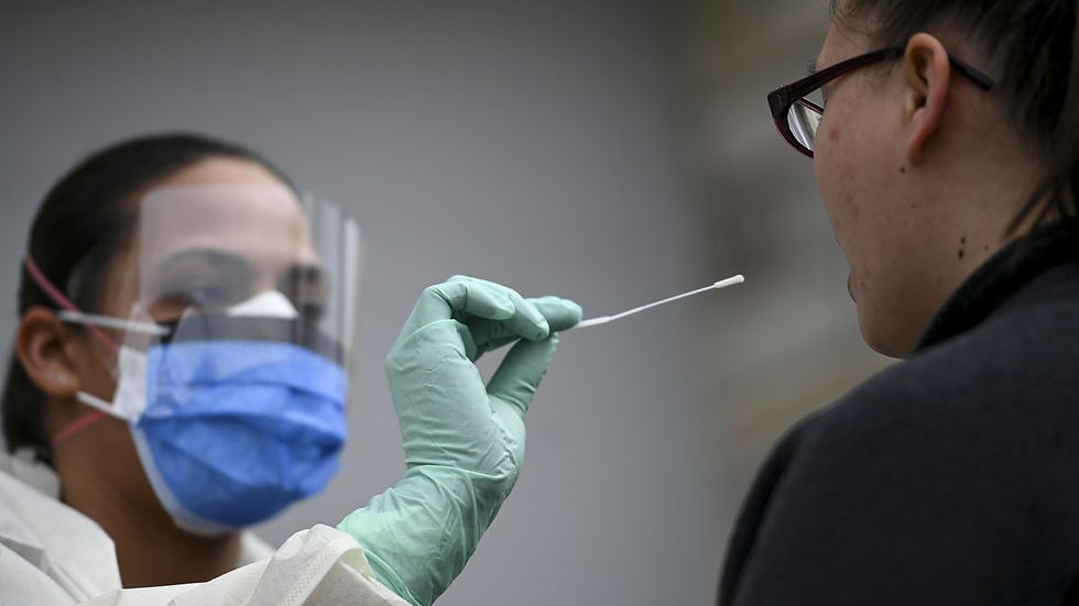
“When only the CDC was doing [tests] in the US,” he said, “we would wait three days, or four, to get a result, which is obviously problematic if you have a patient in the hospital.”
As a teenager, I know what it’s like to be anxious, waiting for the results from a summer program, or a text back. However, the only thing REALLY at stake is my feelings. When it comes to waiting for coronavirus testing results, the tension can be super detrimental.
Your life is on the line!
As a high school student with no knowledge in epidemiology, I can’t say that I know how to eradicate COVID-19. However, as someone with some brand new knowledge of nanotechnology, I can say that maybe there is a way to diagnose the disease without sticking something into your throat and going through the pain of the waiting game.
We can do this by leveraging the power of nanosensors.
What are nanosensors?
Nanosensors are extremely small chemical or mechanical sensors that collect information on the nanoscale and transfer the data for analysis at the macroscopic level.
They are able to detect and communicate information about the behaviour and characteristics of a wide variety of things on the nanoscale: gases, chemical and biochemical species, EM radiation, nanoparticles, and physical measurements such as temperature.
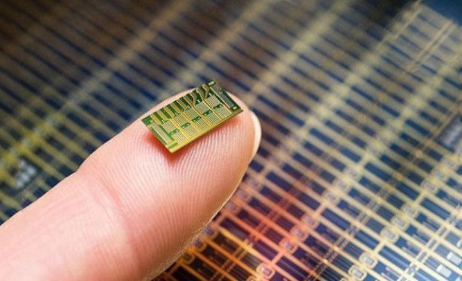
What does that really mean? Well when I say extremely small, I really mean extremely small. Although these sensors are invisible to the naked eye, their capabilities yield an enormous amount of potential in tackling problems.
Because sometimes, to solve the biggest problems, you need to get down to the smallest size.
The prefix nano- deals with objects that have dimensions in nanometres (nm), which is a unit of measurement of 1billionth of a meter. However, that’s way too difficult to visualize on its own. So, I want you to take a piece of paper and try to guess how thick it is in nanometres.
Let's take a piece of paper for comparison:
That piece of paper that you’re holding right now is actually 100,000 nm thick. That’s HUGE… on the nanoscale. For comparison, human DNA is 2.5 nm in diameter. Try to imagine that!
Being so small & microscopic, nanosensors can be much more effective in performing certain tasks and collecting information than traditional sensors for two key reasons:
Firstly, its higher surface area-volume ratio increases the sensor’s sensitivity to a wider variety of variables that it will have to detect, which is crucial since they operate at the same scale as biological processes
Secondly, its ability to monitor things in real-time delivers results FAST, enabling researchers to rapidly analyze data. However, other methods such as spectroscopy actually take days or WEEKS to deliver data.
Basically, nanosensors can detect things that are invisible yet are super important to observe, and allow for much greater efficiency.
But..How do they do that though?
There are two main types of nanosensors:
Chemical nanosensors and Mechanical nanosensors
Both work by detecting changes in the electrical conductivity of a nanomaterial. However, HOW they do it differs.
Chemical nanosensors measure a change in conductivity when the nanomaterial’s usually high conductivity decreases upon binding or absorption (when a solid holds gas, liquid, or solute molecules as a thin film).
On the other hand, mechanical nanosensors measure a change in conductivity when the nanomaterial of the sensor physically changes.
When I was first introduced to the concept of nanotechnology as a kid, I’ve always wondered: how do you build something that small; at the nanoscale?
The answer is nanofabrication.
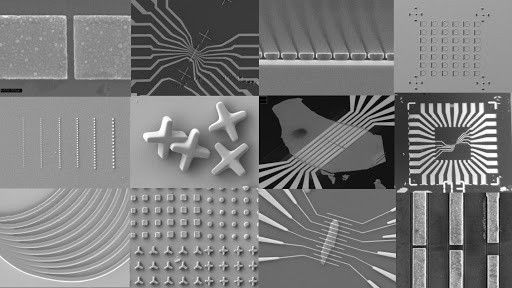
Nanofabrication is the process of designing and building devices with dimensions in the nanoscale (computer engineers especially LOVE this).
There are two types of nanofabrication.
Top-down and Bottom-up
Let’s start with top-down!

Michelangelo's David
Recognize this sculpture? This is Michelangelo’s David — one of the world’s most famous sculptures, an ornate depiction of the human figure, and a perfect example of top-down nanofabrication; otherwise known as lithography.
Before Michelangelo, a sculptor named Agostino di Duccio was faced with a giant block of marble. Eventually, he gave up on trying to sculpt it, leaving it untouched for 10 years. Another sculptor came along — Antonio Rossellino -- and made an attempt at the block, but later decided that it was too difficult to work with.
Eventually, Michelangelo got his hands on this soon-to-be prized piece of marble. After years of chiseling, he was able to transform a giant block into the incredible, towering human figure that stands in museums today.
What does this have to do with top-down nanofabrication? The driving process behind David and lithography is the same. To create David, Michelangelo chiseled away bits and pieces of the marble block and shaped it into a man. Lithography involves removing bits and pieces of material until we get our desired size and shape.
The most common process of lithography for nanofabrication is optical lithography, which uses short-wavelength optical sources such as UV radiation to etch patterns onto a material.
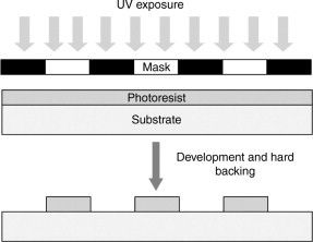
How does optical lithography work?
Imagine painting yourself, shining a lamp onto that painted area, and have the paint MORPH your body.
As creepy as that sounds, that’s essentially how optical lithography works. Also known as photolithography, this process adds a coating whose structure can be manipulated by exposure to light.
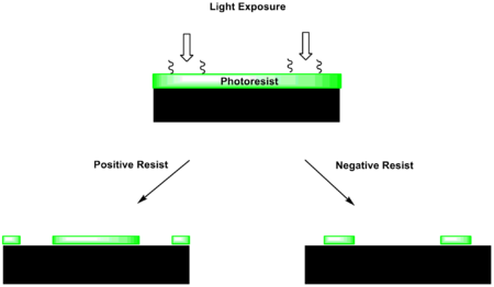
The newly formed pattern is then etched onto the underlying substrate. The coating is called a photoresist. This is an oligomer that sticks onto surfaces and is designed to change its properties when exposed to light. There are two types: a positive resist, and a negative resist.
An oligomer is really just a molecular chain consisting of several repeating chemical units. As you see in the diagram above, light exposure changes the chemical structure of the photoresist in a way that it becomes more liquid-like or soluble.
This is a positive resist. A developer solvent is then used to wash away the polymer to leave behind very fine stencils that are crucial in producing microelectronics.
A negative resist behaves the opposite. Instead of becoming more like a liquid, the polymer will become insoluble when exposed to radiation. This characteristic is key in developing small chips for electronics.
There are plenty of other top-down nanofabrication methods, however. These include:
Electron beam scanning
Nanoimprint scanning
Ion beam scanning
Top-down lithography comes with several problems though.
Environmental pollution; I mean c’mon… you’re shining UV on chemical wafers and washing them away somewhere.
Subtractive method = more costly; the equipment required is more expensive, and of course, the pieces that get taken out of the material are being wasted.
These problems prompt scientists to place a greater focus on bottom-up methods of nanofabrication.
Bottom-up nanofabrication
We’ve all played with LEGOs as a kid! Some people have gone out to build MIND-BLOWING creations like this:

Or uh…things like this:

The possibilities are endless.
What does LEGO have to do with bottom-up nanofabrication? They are both centered around self-assembly. LEGO involves building structures brick by brick, while the bottom-up approach harnesses the properties of molecules to piece together basic units into larger structures of DNA, biopeptides, and more.
We see this process A LOT in nature: DNA assembly, beavers building a dam, etc. In fact, nature — more specifically DNA assembly — has sparked the inspiration for bottom-up approaches in nanofabrication that it is more widely used by scientists when building nanosensors.
One way to design nanosensors using a bottom-up approach is to use liquid-phase techniques based on inverse micelles.
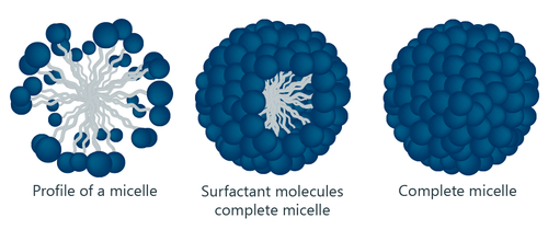
A micelle is a globule of lipid molecules floating in a non-aqueous solution where their hydrophilic ends pointing inwards into the molecule. They play an important role in soaps.
Back to nanosensors → these liquid-phase techniques involving micelles have been developed to form nanoparticles of semiconductors, magnetic, and other materials of various sizes.
There are several advantages to the bottom-up approach:
Decreased likelihood of defects
More homogeneous chemical composition
Improved short and long-range ordering
It’s more cost-effective than top-down, as no materials are wasted. Each building block is an important piece in the puzzle.
However, if you’ve ever tried to complete a giant jigsaw puzzle, you’ll know just how much time it takes. The same goes for bottom-up assembly. Although it makes greater use of materials and costs, it demands more time to design and build nanostructures.
Now we know the pros and cons of each nanofabrication method. We know that the biggest issues with the top-down approach are its environmental ramifications and high cost. The biggest issue with the bottom-down approach is the amount of time it takes.
What if we combined different technologies to tackle these problems and make the nanofabrication process more seamless and efficient?
Some ideas to solve these problems!
Let’s start by tackling the problems caused by the top-down approach. Potentially toxic materials are being washed away during the process. A great way to minimize pollution and waste is to recycle these materials, either through directly re-incorporating them into the design process, or to be used in demonstrations.
The bottom-up approach is being increasingly used by scientists nowadays. Therefore, it’s important to place a greater emphasis on improving these techniques. Here are some ideas to tackle the issue of TIME when constructing nanosensors by combining different technologies:
Quantum computing + AI → design structures on the nanoscale for us!
3D printing → we could design and 3D print the molecular building blocks that we’ll be using in our structures
Back to the pandemic…
I began this article with a grim reminder of the coronavirus pandemic, whose shadow continues to linger over us. However, I also mentioned that I had an idea that involved using nanotechnology to diagnose COVID-19.
When the concept of nanotechnology was first introduced in 1959, people suddenly realized that it was aglow with enormous potential — it would enable us to analyze chemical and biological processes on a level previously impenetrable by scientists.
Introducing… Gold Nanoparticles!
The first attempt at using nanomaterials in virus detection occurred in the late 90s — gold nanoparticles (AuNPs) were combined with silver staining and applied to cervical carcinoma cells in hopes of detecting human papillomavirus.
AuNPs are one of the leading classes of metal nanomaterials. This can be attributed to its versatility and useful characteristics. For starters, AuNPs are widely known for their chemical stability, water solubility, and how easy it is to control their size and shape. Their size ranges from 1–800nm, and they come in all kinds of shapes including but not limited to:
Spheres
Rods
Prisms
Shells
Dog bones (whoa!)
Not only are AuNPs super easy to synthesize, modify their surface, and have outstanding biocompatibility, they are amazing for visualization due to their intense colors. They’re also able to form stable and active bioconjugates with common targeting biomolecules, heightening the sensitivity of detection and allowing researchers to uncover the data they need.
Sounds awesome right?
AuNPs have actually been used to detect SARS — a fellow coronavirus. This is done through 2 main assays:
Colorimetric assay (A) → involves the gold nanoparticles’ ability to choose to absorb single-stranded DNA (ssDNA) over double-stranded DNA (dsDNA). The purpose is to specifically locate viral DNA — the target DNA.
Electrochemical assay (B) → gold nanoparticles are applied to increase electrode conductivity and increase the amount of surface area available for detection probe immobilization.
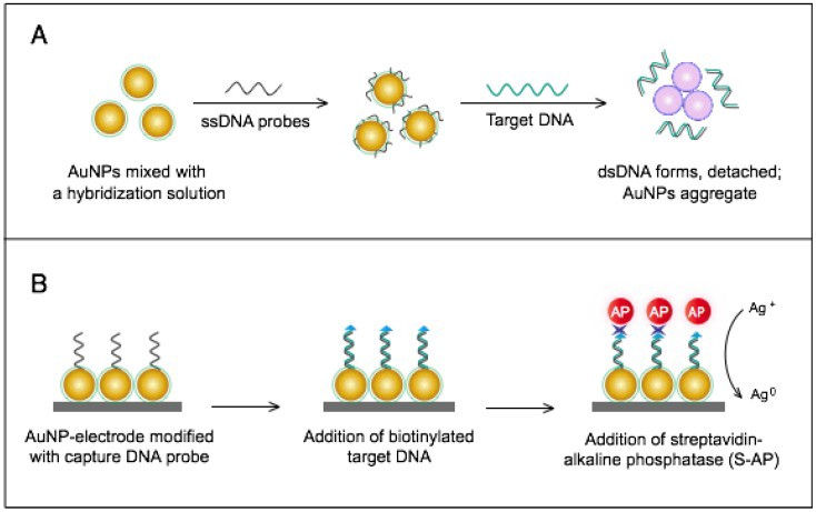
I'll just be talking about colorimetric assays. How this works is actually pretty awesome. Short ssDNA probes will attach themselves to the surface of the gold nanoparticles, which causes 2 key things:
These particles will become more stable in a colloid
These particles will be able to withstand changes in salt levels, without aggregating or changing colour.
Next, the target DNA will attach itself to the ssDNA probes, form dsDNA, detach, leaving the AuNPs to clump together due to the salt. This causes the colour of the solution to turn from red to blue, signifying that, “Hey! We got viral DNA here!”
You can see this change with the naked eye and in 5 minutes, eliminating the need for trained personnel!
This method has been used for SARS. However, with some tweaks, it can be modified to be able to detect COVID-19. In this way, we can turn gold nanoparticles into functional nanosensors that are able to detect the presence of the nucleic acids of a virus.
The detection solution I’m proposing can be boiled down to this: spit into a cup of gold nanoparticles and see if it turns blue.
That is uh… quite questionable, however.

$215?!
Not surprisingly, gold nanoparticles are pricey. There are also some serious challenges in scaling this type of detection method, as well as the logistics behind this solution. After all, no doctor would feel keen about sending expensive chemicals into the hands of ordinary people.
Final Thoughts
Nanotechnology is pervasive in our daily life, and the birth of nanosensors is a pivotal point in the timeline of this emerging technology. Although the idea to diagnose COVID-19 that I presented previously is extremely impractical and will never come into fruition (it may already have been tried), my proposal stands as a testament to the fact that nanosensors are brimming with potential, especially in the medical field. It’s important to continue to find innovative ways to improve upon nanofabrication methods and expand upon the applications that nanotechnology can take on. After all, sometimes, to solve the biggest problems, you need to get down to the smallest size.
Sources:
Draz, Mohamed Shehata, and Hadi Shafiee. “Applications of gold nanoparticles in virus detection.”Theranosticsvol. 8,7 1985-2017. 15 Feb. 2018, doi:10.7150/thno.23856


Comments